
| HOME |
| What is CHIRALTEM |
| 2nd CHIRALTEM workshop |
|
Partner: - Vienna - Regensburg - |
| Publications |
|
|

| Workpackages
Goal: Demonstrate circular dichroism using the
biprism in condenser system. See "Status Quo"<link> for more details.
Goal: Preparation of suitable specimens for
measurements of circular dichroism. Note: I have tried to prepare a specimen of a commercial harddisk, but I did not succeeded yet. The glass plate of the disk is very brittle so it breaks when I grind or polish it to electron transparency. It is also resistant to hydrofluoric acid so it cannot be etched. Any hints for specimen preparation are welcome at petr dot formanek at tu-dresden dot de.
Goal: Optimise experimental setup. |
| Status Quo
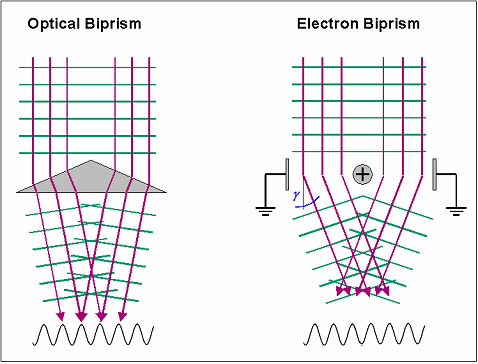
One of the experimental setups, at which circular dichroism can be measured, is realized when a suitable specimen is illuminated by a system of interference fringes with a spacing adapted to the object structure and with a controllable position of the fringes. This is achieved by means of two overlapping coherent electron beams, where the mutual angle of propagation and mutual phase shift has to be controlled. Such an illumination of the specimen can be achieved by placing a biprism into a condenser system of the microscope. The Möllenstedt-type biprism [1] is analogous to the optical biprism (Fig. 1). It consists of a positively biased thin filament (diameter less than a micrometer) placed between two grounded plates. The electric field around the filament deflects the electron waves, so that they interfere below the biprism. The ingenuity of the biprism is that the deflection angle is independent of the distance of the electrons from the filament and that the biprism has virtually no aberrations. The deflection angle is proportional to the voltage Ubp between the filament and the plates with the deflection coefficient dependent on biprism dimensions.
Fig. 1 Principle of biprism operation. where Imax is the maximum and Imin the minimum intensity of the interference fringes.
Fringe spacing, interference width and fringe contrast can be controlled by the distance a of the crossover from the biprism, by the distance b of the image plane from the biprism, and by the biprism voltage Ubp [2] (Fig. 3). where rf is the filament radius, r0 is the effective radius of the emitting area in the electron source, and is the wavelength.
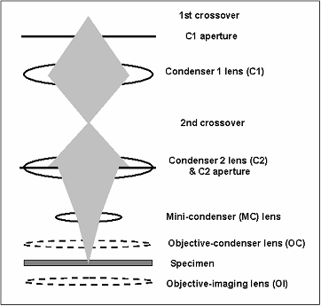
The biprism is placed in the condenser system, which consists of 4 lenses (Fig. 4). By adjusting focal length of the lenses (through varying current in the lenses) and biprism voltage one can (hopefully) adjust S, W, V so that the measurement of circular dichroism is possible.
Fig. 4 Scheme of the condenser system. Although we have a lot of experience with the
biprism mounted below the objective lens for holographic measurements
[2], we presently have only few experiences with a biprism in
the illumination system. We have found several problems that we
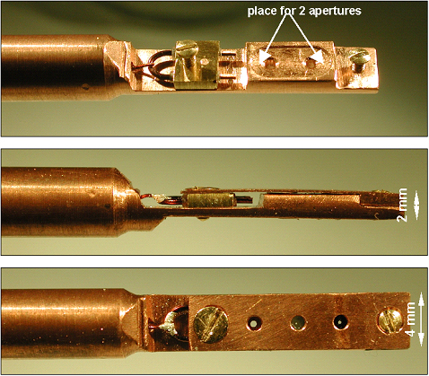
describe further in the following. The standard biprism holder, which is designed to be mounted in the first intermediate image plane (below the objective lens), is too big for the Condenser-2 port of the microscope (above the objective lens) - Fig 5. A down-scaled copy of the standard holder that would fit in a C2 port is hardly manufacturable. Therefore we developed a new construction (Figs. 6 - 8), which can be manufactured in smaller dimensions, and which is in addition more resistant against flashovers [3].
Fig. 5 Comparison of dimensions of a standard C2 aperture holder (top) and standard biprism holder (bottom).
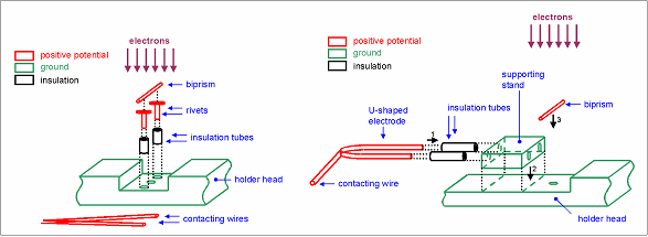
Fig. 6 Comparison of old (left) and new (right)
biprism holder construction.
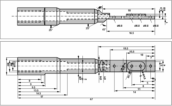
Fig. 7 Technical drawing of the improved biprism holder.
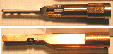
Fig. 8 Photograph of the improved biprism holder.
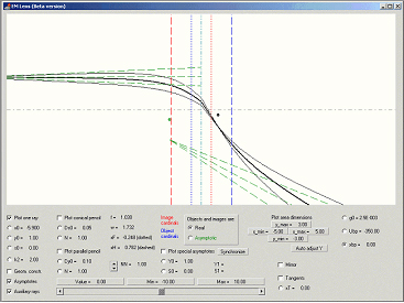
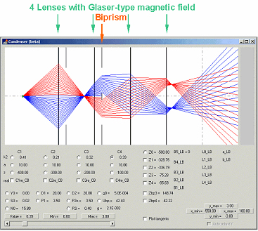
The C2 port of the microscope is placed in the middle of the Condenser 2 lens, i.e. the biprism is placed inside the lens. Since there is no corresponding theory of such a system reported in the literature, imaging properties of a biprism in a lens were calculated [4]<link1>. The conclusion of the calculations is: In an approximation valid for thin lenses and a thin biprism, the system biprism-inside-a-lens is optically equivalent to the system biprism-just-behind-the-lens. In order to better understand the electron optics two programs <link2><link3> were written for live visualization of electron trajectories in a lens and in the system of lenses while varying the parameters of the lenses or of the beam (Fig. 9, 10).
Fig. 9 Screenshot of program visualising beam paths in an electromagnetic lens with a built-in biprism.
Fig. 10 Screenshot of program visualising beam paths in a condenser system.
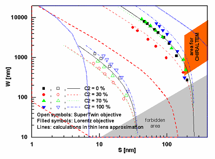
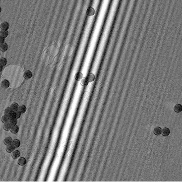
After insertion of the biprism in the C2 port of the microscope and applying a voltage to it, interference fringes with spacings of 5 nm to 40 nm are observable [3]. However, for the measurement of the dichroic signal, fringe spacings of either ~ 0.1 nm or ~ 200 nm are necessary. This could, in principle, be achieved by a corresponding setup of the condenser system, i.e. by deflection angle of the biprism (controlled by the voltage on the biprism), by focal lengths of the Condenser 1, Condenser 2 and Minicondenser lenses (controlled by currents through the lenses), as well as by axially moving the first image of the electron gun - "the crossover" (controlled by gun lens voltage and extraction voltage). This means optimizing 6 parameters is needed. Even though we put a large effort to reach the desirable fringe spacing by varying various microscope parameters, we did not succeed to reach the necessary fringe spacing. It turned out that the condenser system is so complicate that it cannot be adjusted intuitively. We used a model of the system within thin lens approximation (provided by FEI Company), which enabled us to explore all possible setups by brute force method - i.e. just by varying all possible parameters. The result of the simulations and experiments are summarized in Fig. 11. It shows that desired fringe spacing is not achievable in a high-resolution mode of the microscope. The graph in Fig. 11 should be understood as follows. The width of the interference field W is a linear function of the biprism voltage Ubp (Cf. Eq. 3): and the fringe spacing S is indirectly proportional to the biprism voltage (Cf. Eq. 4): These two relationships can be plotted in a W-S diagram (Fig. 11) by the means of a set of parametric curves, the parameter of which is the biprism voltage. The position of a curve is given by the constants A, B, C, which in turn depend on the actual configuration of the condenser system (position of the crossover, excitation of the condenser lenses). By trying all possible combinations of the adjustable parameters, the curve moves in the diagram, filling an area that defines accessible fringe spacings S and interference widths W. The dashed red line in Fig. 11 marks fringe spacings and interference widths achievable with a standard objective lens (SuperTwin lens) and a biprism placed in the second condenser aperture (C2-aperture). It is obvious that this configuration does not allow reaching the desirable fringe spacings. The achievable area would move right-upwards (overlapping the area for the CHIRALTEM), if the biprism were placed in the first condenser aperture (C1-aperture). Since the C1-aperture is placed in the ultra-high-vacuum part of the microscope, any changes must be done by a service engineer. But finally, we found that switching the objective lens off (Low Magnification mode) is a way to approach the desired fringe spacing of ~ 200 nm - the area marked by the blue dotted line in Fig. 11. Optionally, one can use the Lorentz objective lens [6], to win back the degree of freedom that was lost by switching the objective lens off. An image of 200 nm fringes is displayed in Fig. 12.
Fig. 12 Latex spheres of diameter 204 nm on a carbon foil illuminated by two interfering beams with a fringe spacing of about 200 nm.
We would like to express our gratitude to Dr. Peter Tiemeijer from FEI Company for providing the information necessary to progress the project.
[1] G. Möllenstedt, H. Düker, "Fresnelscher Interferenzversuch mit einem Biprisma für Elektronenwellen", Zeitschr. für Physik 42 (1955) 41 [2] M. Lehmann, H. Lichte, "Tutorial on Off-axis Electron Holography", Microscopy and Microanalysis 8 (2002) 447 [3] P. Formanek, B. Einenkel, H. Lichte, "An improved construction of electron biprism holder for the C2-aperture" Proc. Microscopy Conference MC2005, Davos, Switzerland, p. 30 [4] <link1> [5] P. Formanek, B. Einenkel, H. Lichte, "Biprism in condenser system for coherent two-beam illumination of an object", Proc. Microscopy Conference MC2005, Davos, Switzerland, p. 31 [6] J. Zweck, B. Bormans, "The CM30 Lorentz Lens", Philips Electron Optics Bulletin 132 (1992) 1
|
 ,
(2)
,
(2)
 ,
(3)
,
(3) ,
(4)
,
(4) ,
(5)
,
(5)
| Here you find some informations
for download
An improved construction of electron biprism holder for the C2-aperture(PDF) |
||
|
Biprism in condenser system for coherent two-beam illumination of an object(PDF) |
|
|